
Intel's Direct Connect 2025 has given a rundown on what the IFS will work on in the future as the new CEO tries to turn the foundry's momentum around.
Intel Foundry's 14A Process Is Now In Early Testing Stages, Features PowerVia 2.0 & Slated For H2 2026
Well, Intel's new CEO, Lip-Bu Tan, has taken over the stage for the second time since he took over the office, this time at Direct Connect 2025. Jumping into the crux, Intel has revealed an updated foundry roadmap, firstly adding new 18A derivatives, and announcing the enablement of the high-end 14A process. Team Blue claims that they are already working with partners of 14A, sharing early versions of the Process Design Kit (PDK), and based on what we have heard, customers are impressed by Intel's implementation of their next cutting-edge node.

Diving a bit into Intel's 14A process, it is revealed that the node will feature the firm's second-generation PowerVia implementation, called PowerDirect.

This much more power-efficient method focuses directly on supplying and draining transistor power through specialized contacts. So, with 14A, Intel is essentially two generations ahead of TSMC when it comes to employing backside power delivery, which shows that the foundry has plans to dominate the markets moving into the future.
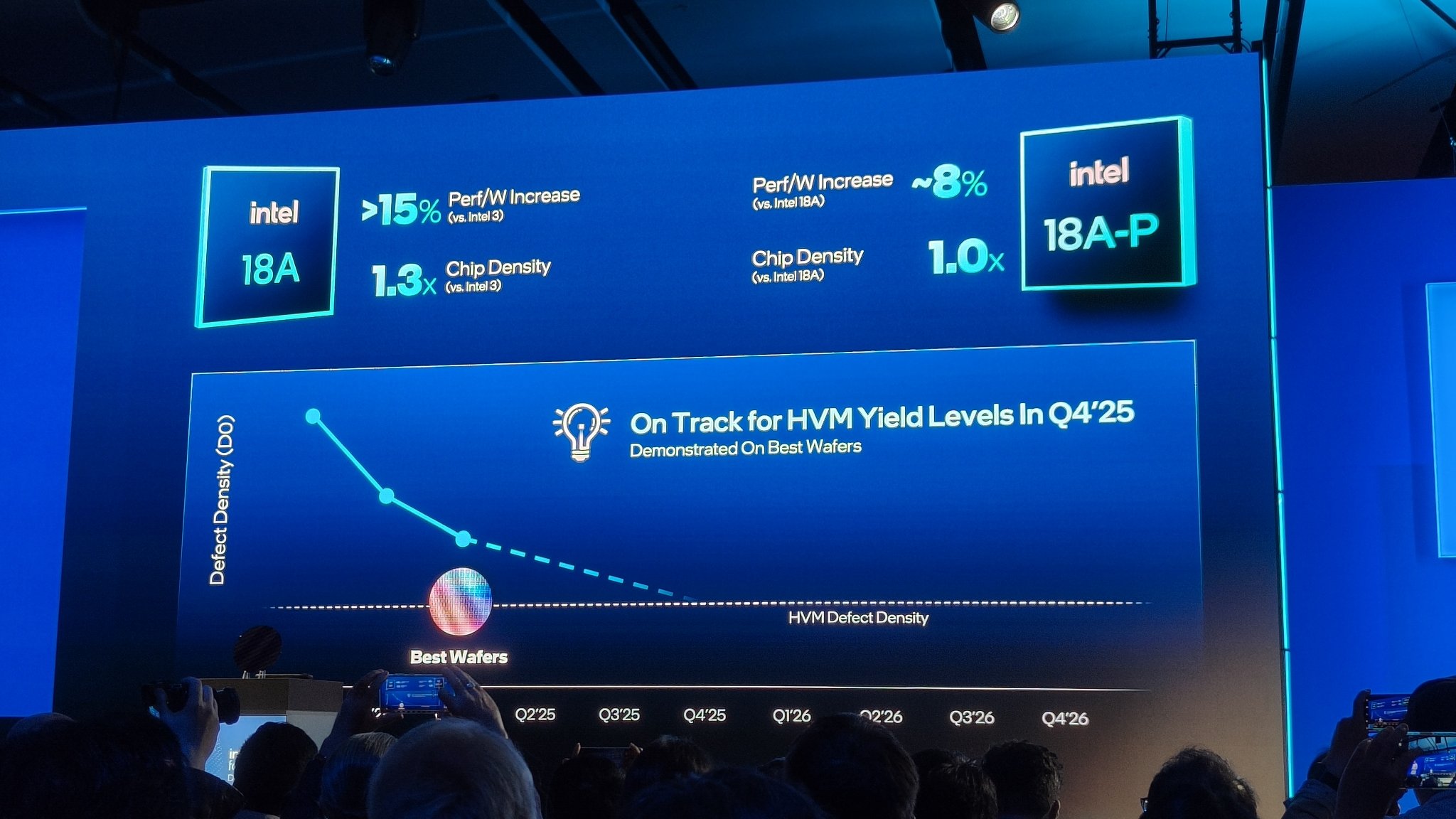
Apart from 14A, the second most significant announcement was probably about the new 18A derivatives, called the 18A-P and 18A-PT. It is claimed that this particular node is a "performance-oriented" process, seeing higher gains than the original node. The more interesting announcement is the 18A-PT, the company's first node to support Foveros Direct 3D hybrid bonding, allowing it to compete with TSMC's interconnect implementations.
The hybrid bonding approach will allow Intel to stack multiple chiplets through TSVs, and it is claimed that the Foveros Direct 3D bonding technology will use a pitch of less than 5 microns, competing against TSMC's SoIC-X approach, which has a 9-micron pitch. This could potentially allow Intel to develop processors similar to AMD's Ryzen X3D CPUs through its in-house nodes, and 18A-PT is already expected to feature with Clearwater Forest Xeon CPUs.


A major announcement included the initiation of risk production for Intel's 18A process, where Team Blue claims that High Volume Manufacturing (HVM) is slated for the end of this year. We have talked about the 18A process several times in the past, but just for a quick rundown, it will be featured on Panther Lake SoCs, which are slated for volume production at the start of 2026. Intel's 18A is a direct counterpart to TSMC's N2, and we expect a surge in competition for cutting-edge nodes in the upcoming times.
EMIB 2.5D
Embedded Multi-die Interconnect Bridge 2.5D
- Efficient, cost-effective way to connect multiple complex die.
- 2.5D packaging for logic-logic and logic-high bandwidth memory (HBM).
- EMIB-M features MIM capacitors in the bridge. EMIB-T adds TSVs to the bridge.
- Silicon bridge embedded in package substrate for shoreline-to-shoreline connection.
- EMIB-T can ease the enablement of IP integration from other packaging designs.
- Simplified supply chain and assembly process.
- Production proven: In mass production since 2017 with Intel and external silicon.
Foveros-S 2.5D
Next generation package optimized for cost/performance.
- Silicon interposer with 4x reticle.
- Applicable in client applications.
- Ideal for solutions with multiple top die chiplets.
- Production proven: In mass production since 2019 with active base die.
Foveros-R 2.5D
Features a redistribution layer (RDL) interposer to create heterogeneous integration between chiplets.
- Applicable for client and cost sensitive segments.
- Ideal for solutions requiring complex function demands from multiple top die chiplets.
- Production ready in 2027.
Foveros-B 2.5D
Combines redistribution layers (RDL) for power and signal with silicon bridges to provide flexible solutions in complex designs.
- Applicable in client and data center applications
- Ideal for solutions with multiple base die chiplets such as cache disaggregation, DVR, or MIM.
- Production ready in 2027.
Foveros Direct 3D
3D stacking of chiplets on active base die for superior power-per-bit performance.
- Cu-to-Cu hybrid bonding interface (HBI).
- Ultra-high bandwidth and low power interconnect.
- High density and low resistance die-to-die interconnect.
- Applicable in client and data center applications.
- Foveros Direct stacks enabled on EMIB 3.5D solutions.
EMIB 3.5D
Embedded Multi-die Interconnect Bridge 3.5D and Foveros in one package.
- Enables flexible heterogeneous systems with a wide variety of dies.
- Well-suited to applications where there is a need to combine multiple 3D stacks in one package.
- Intel® Data Center GPU Max Series SoC: using EMIB 3.5D to create Intel’s most complex heterogeneous chip ever mass-produced with more than 100 billion transistors, 47 active tiles, and 5 process nodes.
With 20A being cancelled, Intel Foundry is now focused on creating a foundry ecosystem in collaboration with partners, since Tan's keynote emphasized customer relations. The IFS is working with the likes of Synopsys and Cadence to ensure that its nodes are according to industry demands, and partner sampling is the way through which Team Blue could see a massive improvement in foundry performance.

About the author: Muhammad Zuhair is a hardware and technology reporter for Wccftech, specializing in the semiconductor industry and the complex interplay between technology, manufacturing, and geopolitics. His coverage focuses on the corporate strategies and technological roadmaps of industry giants like TSMC, NVIDIA, Samsung, and Intel. Zuhair's expertise lies in deconstructing complex topics such as fabrication nodes (e.g., 2nm process), the economic impact of policies like the CHIPS Act, and the strategic development of AI infrastructure from NVIDIA, AMD and Intel.
Follow Wccftech on Google to get more of our news coverage in your feeds.


