


Samsung Foundry has announced that they have secured a 2nm order from a Japanese firm, snatching away TSMC's well-established customer.
Samsung's 2nm Process Is a Testament To the Commitment They Have Towards The Semiconductor Division
The Korean giant disclosed the development in a press release, which isn't ordinary because 2nm is still a process that hasn't made it into mainstream markets. Samsung securing a client shows that not only is the company's 2nm node sufficient for market adoption, but Samsung is looking to close the gap with the Taiwan semiconductor giant TSMC. With the 2nm, the competition does look to narrow down.
This order is pivotal as it validates Samsung’s 2nm GAA process technology and Advanced Package technology as an ideal solution for next-generation AI accelerators. We are committed to closely collaborating with our customers ensuring that the high performance and low power characteristics of our products are fully realized.
- Taejoong Song, Corporate VP at Samsung Electronics
Samsung's "publicly disclosed" 2nm customer is Preferred Networks, a leading Japanese AI company. The firm is heavily involved in R&D work, focusing on deep learning research and development (R&D). Interestingly, we reported on this rumor a few months ago, when local outlets reported a potential partnership between Preferred Networks, but now, the deal looks to be officially secured.
Preferred Networks is now moving towards vertically integrating "the AI value chain from chips to supercomputers," which provides a medium for businesses to have their own AI clusters. The Japanese firm has become the first in the region to utilize such a process, marking a breakthrough for the nation and Samsung.
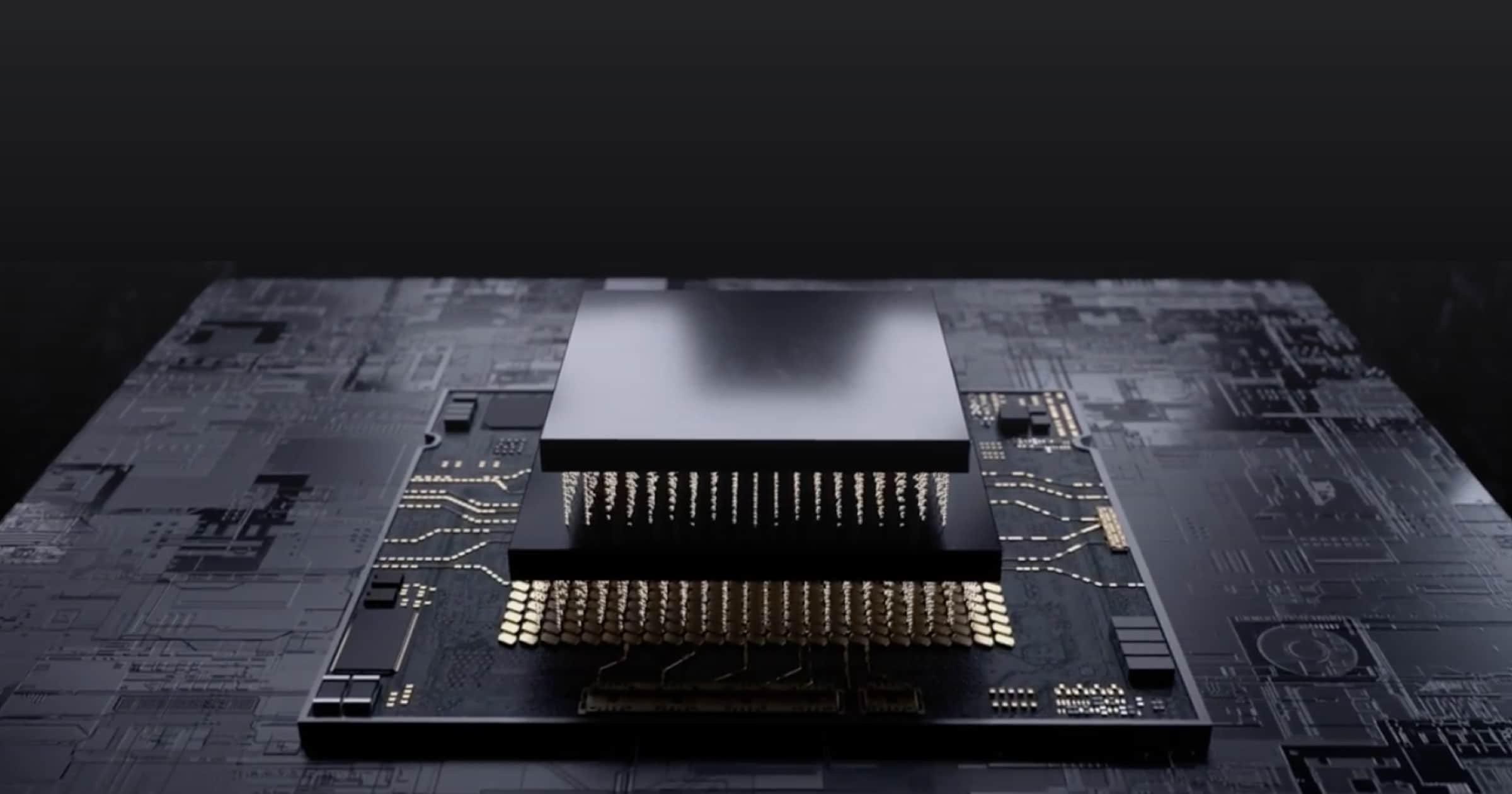

Apart from 2nm, Preferred Networks looks to utilize Samsung's 2.5D packaging technology, the Interposer-Cube S, yet again showing that the Korean giant's packaging services are not less than those of other competitors. It was rumored previously that Samsung supplied 2.5D packaging to NVIDIA for their Hopper generation as well. While Samsung hasn't faced the exposure with its packaging facilities compared to the likes of TSMC, they certainly look on the right track.
In terms of the 2nm process in general, we recently reported that the Taiwan giant TSMC plans to initiate trial production of the node by next week. Apple and NVIDIA are major customers. Mass production is slated for 2025, which means that the node will be integrated into mainstream market products by either Q1 2025 or the next quarter.
News Source: Samsung Newsroom

About the author: Muhammad Zuhair is a hardware and technology reporter for Wccftech, specializing in the semiconductor industry and the complex interplay between technology, manufacturing, and geopolitics. His coverage focuses on the corporate strategies and technological roadmaps of industry giants like TSMC, NVIDIA, Samsung, and Intel. Zuhair's expertise lies in deconstructing complex topics such as fabrication nodes (e.g., 2nm process), the economic impact of policies like the CHIPS Act, and the strategic development of AI infrastructure from NVIDIA, AMD and Intel.
Follow Wccftech on Google to get more of our news coverage in your feeds.


