


When we talk about computer memory nowadays, most people think of “RAM” or perhaps the long-term storage in their phones or laptops. But behind those simple terms lies a vast and fascinating ecosystem of semiconductor memory technologies, each with its own history, design philosophy, and role in modern electronics. At its core, memory in computers stores information, from the instructions and data a processor is actively using to the massive amounts of user content and system files we keep on our SSDs and memory cards. Yet not all memory is created equal in how fast it responds, how long it retains data, or how much it costs per gigabyte.
This article will focus on four types of modern computer memory: Read-Only Memory (ROM), Dynamic Random Access Memory (DRAM), Static Random Access Memory (SRAM), and flash memory. Each of these memory types represents a distinct point in the trade-off space between speed, cost, power, and persistence. Understanding these trade-offs is essential not only for hardware engineers but for enthusiasts, overclockers, storage space hunters, and anyone seeking to optimize performance, make informed buying decisions, or simply wanting to learn about the technology powering their computers.
This article doesn’t just break down what these memories are and how they work. It explores why they matter, how they’ve evolved over decades of innovation, and what practical implications their strengths and weaknesses have for systems ranging from gaming PCs to data centers to smartphones. Whether you’re trying to decide between various DDR5 memory kits, understand why your SSD slows down with use, or simply grasp how modern computing orchestrates the flow of data at blazing speeds, the interplay between the various computer memory types is where the story begins.
What Is Memory, Fundamentally?
At its core, computer memory is the part of a computing system that stores information in the form of binary digits (bits) either for active use by the processor or other system components, such as Graphics Processing Units (GPUs), or for long-term storage at the behest of the user. But the term "memory" actually covers a wide range of technologies with very different characteristics, performance profiles, and roles in a modern system.
Memory isn’t just one box that holds data; it’s part of a hierarchical ecosystem designed to balance speed, capacity, cost, and persistence, simply because no single technology can be fast, cheap, large, and durable all at once.

The Two Fundamental Memory Classes: Volatile vs. Non-Volatile
One of the most basic ways memory is categorized is by whether it retains data when power is removed:
Volatile memory
This type of memory requires continuous electrical power to maintain the stored bits. Once power is cut, the data are simply lost. Because of this behavior, volatile memory is typically used for temporary storage where speed is critical. Volatile memory contains two main sub-groups: Dynamic Random Access Memory (DRAM) and Static Random Access Memory (SRAM), and we shall explore both in detail later on.
Non-volatile memory
In non-volatile memory, data persisteven without power. This makes this type of memory suitable for long-term storage and systems where preserving information across power cycles is essential. Examples of non-volatile memory include Read-Only Memory (ROM), magnetic disks, optical media, and flash memory.
Beyond Volatility: Access Patterns & Performance
A second fundamental idea is how memory is accessed:
- Random Access: Any memory location can be read or written in roughly equal time. The “R” in RAM stands for this property;
- Sequential Access: Data must be read in order, which is slower for arbitrary access. Hard disk drives and old tape storage are examples of this, even if bits are ultimately stored on non-volatile media.
Memory Hierarchy: Why Multiple Types Exist Together
Modern computing doesn’t rely on just one memory type but organizes several of them into a hierarchy:
- Registers: Ultra-tiny, super-fast SRAM storage inside a Central Processing Unit (CPU) core, or a GPU/Tensor Processing Unit (TPU)'s compute units;
- Cache Memory: Very fast SRAM placed close to a processor to buffer frequently accessed data;
- Main Memory (DRAM): Larger and slower than a cache, serving as the processor’s main working set;
- Non-Volatile Storage: High-capacity, slower devices used for long-term storage like operating system files, applications, games, and personal files.
This hierarchy exists because processor speeds have historically advanced much faster than memory speeds. Without layering different types of memory with different costs and performance traits, CPUs would often sit idle waiting for data, which is a phenomenon called the “memory wall”.
Core Properties That Define Memory
When engineers design or compare memory technologies, they look at several fundamental metrics:
- Speed: How quickly data can be read from or written to memory;
- Latency: The delay between a request and the start of data transfer;
- Bandwidth: The amount of data that can be moved per unit of time;
- Capacity: How much data can be stored;
- Cost per bit: How much each unit of storage costs to produce;
- Persistence: Whether the stored data survives a loss of power;
- Energy Usage: Affects battery life and heat output, especially in smaller devices;
No memory type excels in all metrics at once, and that’s exactly why modern computers combine various types of memory instead of relying on one universal solution.
Note: While modern computer memory actually stores data in the form of bits at the lowest, physical level, some of its characteristics are usually expressed in bytes, which are collections of eight bits.
Why This Matters in Everyday Systems
- Program execution: When you launch an application, it typically gets loaded from slower, non-volatile storage into fast, volatile memory so that the CPU can manipulate it as quickly and as efficiently as possible;
- Caches: Modern CPUs exploit data locality — recent or nearby data is more likely to be reused — by storing it in extremely fast SRAM-based caches so that repeated accesses don’t incur DRAM’s higher latency penalty;
- Long-term storage: Your various files, games, and other miscellaneous data are stored on non-volatile memory (such as NAND flash memory) precisely because it retains data without power, even if that comes at a performance cost when compared to RAM.
In what follows, we will be exploring the characteristics, use cases, strengths, and weaknesses of the four main types of modern computer memory that this article will cover, starting with Read-Only Memory (ROM).
ROM — Read-Only Memory
In the modern computing world, Read-Only Memory (ROM) refers to a broad class of non-volatile memory technologies designed to retain data even when power is removed. Unlike volatile memory — which loses its stored data upon power loss — ROM historically held fixed data or firmware that a given system needed to start up and operate correctly, such as boot code, microcode, or embedded controller instructions.
While modern production often blurs the line between “read-only” and “rewriteable” memory, understanding the classic ROM subtypes — and how they evolved — helps explain everything from early game cartridges to firmware storage in modern PCs and smartphones.

ROM’s primary role is to store critical, long-lived data reliably:
- It’s non-volatile, so its contents persist through power cycles;
- Firmware and bootloaders — including BIOS/Unified Extensible Firmware Interface (UEFI) on modern PCs — traditionally reside in ROM;
- Many embedded systems (from appliances to controllers) rely on ROM for stable on-board software.
Except for a few specialized systems, ROM isn’t meant to be rewritten frequently. But over time, various subtypes evolved to offer different degrees of flexibility. We shall explore their strengths, weaknesses, and typical use cases in what follows.
Classic ROM Subtypes
Here are the major categories of ROM, ranging from permanently fixed to electrically rewriteable:
Mask ROM (MROM) — Factory Programmed, Unchangeable
Mask ROM is programmed during manufacturing, as the data pattern is physically embedded on the chip using custom photomasks. Because the bits are “hard-wired” at the factory, they cannot be altered afterward.
Strengths
- Very stable and fast to read;
- Cost-effective at massive production scales because the custom mask step replaces post-manufacturing programming.
Weaknesses
- Inflexible, as any change requires a new mask and chip fabrication pass;
- Rare in small-volume or frequently updated products.
Typical use cases
- Early game cartridges and console ROMs;
- Embedded systems with fixed code.
Programmable ROM (PROM) — One-Time Programmable
PROM is manufactured blank and can be programmed once by the user using a special device called a PROM programmer. During programming, internal fuses are selectively “burned” to define stored bits. Once programmed, the data cannot be changed.
Strengths
- Enables custom programming without custom masks;
- Useful when a firmware image needs to be baked into a circuit late in the manufacturing chain.
Weaknesses
- Only programmable once; mistakes often mean discarding the chip.
Typical use cases
- Industrial embedded systems, early test systems, or application-specific logic.
EPROM (Erasable Programmable ROM) — Ultraviolet (UV) Light Erasable
EPROM improved on PROM by allowing the contents to be erased and reprogrammed. Erasure is accomplished by exposing the chip (through a transparent quartz window in its package) to strong ultraviolet light, thus resetting the floating-gate transistors.
Strengths
- Reusable, as programmers could iterate on firmware during development;
- Good for prototyping and legacy BIOS chips.
Weaknesses
- Erasure requires removal of the chip and UV exposure, making updates inconvenient in deployed products;
- Erase cycles limited by UV window wear.
Typical use cases
- Early microcontroller firmware and development boards.
EEPROM (Electrically Erasable Programmable ROM) — Electric Byte-Level Erasable
EEPROM allows both erasing and reprogramming electrically, without removing the chip from the circuit. This makes it much more convenient than EPROM.
Unique characteristics
- Can selectively erase and rewrite individual bytes, unlike flash memory, which typically works in blocks;
- Slower write speeds than RAM, but more flexible than EPROM.
Strengths
- In-system update capability (e.g., via SPI or I²C busses);
- Useful for small firmware updates or configuration data.
Weaknesses
- Write endurance is finite (often tens of thousands to millions of cycles).
Typical use cases
- BIOS/UEFI firmware storage on modern motherboards;
- Microcontroller embedded systems;
- Security tokens and smart card storage.
Summary: How the various ROM types compare
| Type | Programmable? | Reprogrammable? | Erase Method | Typical Use Case |
|---|---|---|---|---|
| Mask ROM | No | No | N/A | Mass-produced embedded firmware |
| PROM | Yes (once) | No | Fuse burn | Custom firmware in stable devices |
| EPROM | Yes | Yes | UV light | Legacy firmware development |
| EEPROM | Yes | Yes | Electrical (byte) | BIOS, microcontrollers, config storage |
DRAM — Dynamic Random-Access Memory
Dynamic Random-Access Memory (DRAM) is the dominant form of main memory in computing systems today. It stores data using tiny capacitors that hold charge, with each bit requiring occasional refresh cycles because the charge slowly leaks away. This “dynamic” nature is what gives DRAM its name — it must be regularly refreshed hundreds of times per second to retain information. Because DRAM cells are simpler than those used in SRAM, DRAM achieves far higher density per chip, making it far more cost-effective for large memory capacities. This balance of cost, performance, and density is why DRAM is used as the main workspace for applications and operating systems in devices from PCs to servers and beyond.
In terms of how it works, DRAM cells store a single bit of data using one small capacitor paired with one access transistor. These cells are organized in a 2-dimensional grid of rows and columns, and each cell sits at the intersection of a word line (row) and a bit line (column).
- The word line acts as a selector for an entire row of cells. When the memory controller wants to access a row, it drives that word line high, which turns on the access transistors for all cells in that row so they connect to their corresponding bit lines;
- The bit lines run down each column and serve as the path for data transfer between the cell’s capacitor and the sense amplifiers. During a read operation, the bit line is first pre-charged to an intermediate voltage, then the word line is activated. The tiny charge stored on the cell’s capacitor slightly alters the bit line’s voltage, and the sense amplifier detects and amplifies this difference to produce a logical (“1” or “0”) value. For a write operation, the bit line is driven strongly to the desired logic level, and the word line is activated so the capacitor is charged (for a 1) or discharged (for a 0).
Because the stored charge on the capacitor leaks over time and because reading actually disturbs the cell’s stored charge, modern DRAM must refresh its contents periodically by re-reading and re-writing each row to preserve its data.

DRAM’s Main Characteristics
Strengths
- High density at reasonable cost: DRAM stores more bits per unit area than SRAM and is much cheaper per gigabyte, making it ideal for main memory;
- Good general-purpose speed: While slower than some specialized variants, DRAM provides excellent bandwidth for a wide range of workloads;
- Highly standardized: Multiple DDR generations are widely supported across desktops, laptops, and servers.
Weaknesses
- Needs refresh cycles: Because it uses charge to store data, DRAM periodically consumes extra power just to maintain contents;
- Volatile: Like SRAM, DRAM loses all stored data when power is removed;
- Latency limitations: While overall throughput is strong, data access latency (especially during random access) is much higher compared with SRAM.
Typical use cases
- System/device memory in desktops, laptops, phones, servers, etc.;
- General-purpose workloads where capacity and cost matter;
- Virtualization, large datasets, and most everyday computing tasks.
Memory Buses — How Data Get Around

In a computing system, a bus is essentially a set of electrical pathways that transfers information between different components, like the CPU, memory, and other devices. A memory bus specifically connects the processor — precisely the memory controller inside the processor — to the system’s memory, enabling data and instructions to move between the CPU and DRAM or other memories. In modern designs, this connection is typically defined by memory standards and implemented as a high-speed interface so that the CPU can read or write memory quickly and efficiently.
A memory bus is made of several logical sub-buses:
- Address bus: Carries the addresses of the memory locations the CPU wants to access (e.g., “read the byte at address 0x12345”). The width of the address bus influences how much memory the system can address;
- Data bus: Transfers the actual data between memory and the CPU. Wider data buses allow more bits to be moved in each transfer, increasing overall throughput/bandwidth;
- Control bus: Carries control signals (such as read or write commands) that coordinate when and how data moves.
Together, these buses form the communication “highways” over which memory operations occur. The width (number of parallel lines) and speed (frequency) of a memory bus directly impact how much data can be moved per unit of time (AKA memory bandwidth), which is similar to how a wider and faster highway can carry more cars.
In modern systems, the traditional front-side memory bus has evolved into more specialized, point-to-point memory interfaces integrated into CPU memory controllers and defined by standards like DDR, LPDDR, GDDR, and HBM, but the same basic principles — addressing, data transfer, and control over defined physical lines — still apply.
DRAM Vs SDRAM — A Short Clarification
Although we use the term DRAM broadly to describe the main memory in today’s computers, it’s important to understand that virtually all modern DRAM chips are actually SDRAM — Synchronous Dynamic Random-Access Memory. SDRAM differs from older, asynchronous DRAM in that its command and data operations are tightly coordinated with a system clock signal, meaning the memory controller — a digital circuit that manages the flow of data going to and from a computer's main memory — and the DRAM chips operate in lock-step with each other. This synchronization enables features like command pipelining and bank interleaving, which greatly increase throughput and efficiency compared to the asynchronous DRAM interfaces of the past. In fact, all DRAM variants, such as DDR, LPDDR, GDDR, and even HBM, are all SDRAM-based at their core, as they simply build on that synchronous foundation with additional enhancements for bandwidth, latency, energy efficiency, or specialized use cases.
Memory Timings

When you see a memory spec like "30-36-36-76" on a DDR5 DRAM kit, for example, that string of numbers refers to the kit’s primary memory timings, which essentially represent the number of clock cycles the memory needs to perform certain key operations. Because DRAM is organized as a grid of rows and columns, accessing data involves activating a row and then reading or writing a column within it, and these operations introduce measurable delays. The most commonly cited timings are:
- CAS Latency (tCL): The number of clock cycles between a read command and when the data actually becomes available, once the correct row is already active. This is the most familiar number to enthusiasts and is often used as shorthand for memory responsiveness;
- Row-to-Column Delay (tRCD): The delay between activating a row and accessing the desired column within that row, which is essentially the time to get from row setup to column access;
- Row Precharge Time (tRP): Before switching to a different row, the current row must be “precharged” (closed), and tRP defines how many clock cycles that operation takes;
- Row Active Time (tRAS): The minimum number of clock cycles a row must remain active after being opened before it can be safely closed again.
Lower numbers indicate fewer clock cycles and typically correspond to lower latency, but the real-world delay also depends on the DRAM frequency, as a lower timing number at a slower clock speed can have similar actual latency (usually expressed in nanoseconds) to a higher timing number at a faster frequency.
Most memory modules are designed with a balance between high transfer rates and reasonable timings. Enthusiasts tuning performance sometimes adjust these values or consider them when evaluating kits, since they influence how quickly a DRAM module can respond to memory requests beyond raw bandwidth.
It’s worth noting that the familiar primary timings (like tCL, tRCD, tRP, and tRAS) don’t tell the whole story when it comes to memory performance. Beneath them lie secondary and tertiary timings, which represent additional delay parameters that govern more nuanced aspects of how DRAM responds to different command sequences and refresh cycles. These subtimings aren’t typically listed on packaging but can often be accessed and adjusted in a computer's BIOS/UEFI, and properly tuning them can have a much larger impact on memory bandwidth and latency, compared to just tweaking primary timings. Enthusiasts in the PC community commonly explore these settings as part of memory tuning and overclocking, squeezing out extra performance once the basic timing and frequency targets have been met.
The following are four of the major DRAM flavors you’ll encounter in modern systems, each optimized for different performance/power/cost priorities and environments.
DDR — Double Data Rate (Standard System Memory)

DDR (Double Data Rate) DRAM represents the mainstream system memory used in today's desktops, laptops, workstations, and servers. It transfers data on both the rising and falling clock edges, effectively doubling the data rate per clock cycle compared with older Single Data Rate (SDR) DRAM. DDR has evolved through multiple generations (from DDR1 to DDR5, and soon DDR6), with each subsequent generation improving speed/frequency, capacity, and energy efficiency.
Strengths
- Balanced performance: Good overall bandwidth, latency, and capacity for general applications;
- Widely supported and upgradable: DDR comes in standardized modules (like DIMMs) that are easy to install or upgrade in many systems;
- Cost-effective: Mature manufacturing and wide adoption keep prices competitive. Also much cheaper and denser than SRAM.
Weaknesses
- Moderate power usage: Not as energy efficient as the mobile-oriented LPDDR;
- Bandwidth and latency constraints: Much higher data access latency and much lower bandwidth than SRAM.
Typical use cases
- Main system memory in consumer and enterprise desktops, laptops, and servers.
LPDDR — Low-Power DRAM (Mobile & Embedded DRAM)

Low-Power DDR (LPDDR) memory is specifically tailored for battery-powered and mobile devices, such as laptops, smartphones, and tablets. While it uses the same fundamental DRAM technology as standard DDR DRAM, LPDDR memory is optimized for lower voltage operation and is equipped with extra power-saving modes. It is often soldered directly onto device logic boards rather than in user-swappable modules, enabling smaller designs and reduced power consumption in thin laptops, smartphones, and tablets.
Strengths
- Excellent energy efficiency: Designed to operate at lower voltages for better battery life;
- Optimized for always-on, low-power states: Good performance for mobile workloads without draining power;
- Smaller form factors: Soldered designs reduce board space and complexity.
Weaknesses
- Not upgradeable: LPDDR is usually soldered down and cannot be user-replaced like standard DDR;
- Higher latency: Compared to DDR DRAM, LPDDR memory latency is usually quite a bit higher, due to looser memory timings.
Typical use cases
- Smartphones, tablets, ultra-portable laptops, automotive systems.
GDDR — Graphics DRAM (High-Speed Graphics Memory)

Graphics DDR (GDDR) memory is a specialized variant of DDR DRAM that's designed to deliver higher peak bandwidth for graphics and "embarrassingly parallel" workloads. With wider buses and higher clock speeds, GDDR (e.g., GDDR6, GDDR7) provides the significant throughput needed for video game rendering and other bandwidth-intensive compute tasks. It trades some power efficiency for raw speed, making it suitable for GPUs and other parallel compute accelerators where memory bandwidth directly impacts performance.
Strengths
- Very high data rates: Designed to push large amounts of data rapidly between the GPU and memory;
- Well-optimized for parallel workloads: Works well with multiple memory channels to maximize throughput.
Weaknesses
- Heat and power: The high operating frequency and wider memory buses can lead to increased heat generation and power draw;
- Not designed for general-purpose memory: Trade-offs favor bandwidth over latency or flexibility.
Typical use cases
- Graphics cards/GPUs, gaming consoles, and professional visualization hardware.
HBM — High Bandwidth Memory (Top-Tier Bandwidth for High-Performance Computing)

High Bandwidth Memory (HBM) represents a 3D-stacked approach to DRAM that dramatically increases memory bandwidth per package. Using Through-Silicon Vias (TSVs) and an ultra-wide bus, HBM delivers massive throughput with much lower power per bit transferred compared with DDR and GDDR. It’s typically paired directly with high-performance GPUs, AI accelerators, or any other High-Performance Computing (HPC) processors via an interposer, which is a thin intermediary substrate that enables extremely dense, high-speed connections between the processor and the memory stacks, routing thousands of signals with minimal latency and power loss.
In HBM systems, the processor die and one or more stacked DRAM dies sit side-by-side on this interposer in a 2.5D package, which provides ultra-fine wiring and micro-bump connections that would be impractical to achieve on a regular PCB. The result is the wide, high-bandwidth interface HBM is known for — short interconnect paths between a compute-focused chip and memory that support massive throughput and improved energy efficiency compared with traditional off-chip memory routing.
Strengths
- Unmatched bandwidth per stack: Can reach hundreds of gigabytes per second per package;
- Impeccable energy efficiency: Lowers energy usage (usually expressed in picojoules per bit) compared with traditional DDR/GDDR designs;
- Dense, compact form factor: 3D stacking saves space and enables high-performance boards.
Weaknesses
- Very high cost and complexity: 2.5D/TSV packaging and interposers add extra manufacturing expenses;
- Limited capacity vs standard DRAM: Focused on high throughput over sheer size.
Typical use cases
- AI accelerators (GPUs and TPUs) and HPC.
Summary: Comparison of DRAM Types
| DRAM Type | Primary Goal | Strengths | Weaknesses | Common Uses |
|---|---|---|---|---|
| DDR | Balanced system memory | Cost-effective, general-purpose | Moderate bandwidth | Desktops, laptops, servers, etc. |
| LPDDR | Energy efficiency-optimized memory | Excellent energy efficiency | High latency, non-upgradeable | Smartphones, tablets, ultraportables, etc. |
| GDDR | High throughput-optimized memory | Very high bandwidth | High power draw & heat | GPUs |
| HBM | Extreme bandwidth memory | Massive throughput & energy efficiency | High cost & packaging complexity | AI/HPC accelerators, TPUs, etc. |
SRAM — Static Random-Access Memory
Static Random-Access Memory (SRAM) is a form of volatile memory but it occupies a very special place in modern computing due to its speed, predictability, and ease of use. While it’s not the largest or cheapest type of memory, SRAM’s unique characteristics make it indispensable in systems where performance is paramount, even if it comes at a considerable cost in other areas.

What SRAM Is and How It Works
Unlike DRAM, which stores bits as electrical charge in a capacitor and requires periodic refresh cycles, SRAM uses a network of transistors configured as flip-flops to hold each bit of data. A typical SRAM cell uses six transistors per bit (often described as a 6T cell), which can latch a stable 0 or 1 as long as power is supplied, without the need for refresh operations.
This “static” nature is why SRAM is called Static RAM: once a bit is written, it stays there statically until it is explicitly overwritten or power is cut.
Key Characteristics of SRAM
SRAM’s design gives it a distinct set of performance traits:
- Fast access times: SRAM can deliver reads and writes in single-digit nanoseconds, which is an order of magnitude faster than DRAM’s tens of nanoseconds;
- No refresh needed: Because bits are held in flip-flops rather than charge, SRAM doesn’t require refresh cycles, which greatly reduces latency and energy spent on background maintenance;
- Low dynamic power consumption: Without refresh overhead, SRAM generally consumes less dynamic power during frequent accesses, which is a big boon in caches and high-speed logic;
- Predictable timing: The absence of unpredictable refresh activity gives SRAM deterministic latency, which is crucial for real-time applications;
- Volatile: Like most RAM types, SRAM loses all stored data when power is removed.
Strengths of SRAM
High speed and low latency: SRAM’s transistor-based cells make it one of the fastest memory technologies in common use, as it provides near-instant access to stored data. This is why it’s ideal for applications that demand rapid responses from memory.
No refresh overhead: Unlike DRAM, which must pause for refresh cycles, SRAM retains data statically and doesn’t need that extra circuitry or power drain.
Efficient for performance-critical logic: In many computing systems, SRAM’s predictable timing and quick access translate to better overall throughput, especially where consistent performance matters most.
Lower idle power: In read-intensive workloads and idle scenarios, SRAM can consume less power overall than DRAM because there’s no constant refreshing.
Weaknesses of SRAM
High cost per bit: Because each SRAM cell uses multiple transistors to store just one bit, SRAM is much more expensive to manufacture than DRAM or flash memory. This makes it impractical for applications that require large amounts of storage.
Low density: The multi-transistor cell structure means SRAM occupies more silicon area per bit, resulting in lower storage density and larger die sizes for the same capacity compared to DRAM.
Volatility: Like other RAM types, SRAM doesn’t retain data without power, so it can’t be used for long-term data storage without supplemental battery or backup mechanisms.
Power in deep processes: While SRAM avoids refresh overhead, advanced low-leakage processes (e.g., deep-submicron designs) can still have standby leakage currents that diminish some of its energy benefits.
Typical Use Cases
Because of its combination of speed and predictability, SRAM finds its home in areas where performance is more important than capacity:
- CPU and GPU cache memory: SRAM is the preferred memory type for L1, L2, and L3 caches, sitting closest to the processor cores to minimize data access latency;
- Register files and small buffers: Small, high-speed local memories inside processors and specialized logic blocks often use SRAM;
- Real-time and embedded systems: When timing determinism matters — such as in networking equipment or control systems — SRAM’s lack of refresh cycles and low latency are huge advantages;
- High-speed networking hardware: Packet buffers in routers and switches frequently use SRAM to quickly queue and forward network traffic;
- ASIC/FPGA block RAM: Many Application-Specific Integrated Circuits (ASICs) such as Field-Programmable Gate Arrays (FPGAs) embed SRAM blocks as configurable on-chip/scratchpad memory for flexible logic designs.
In Summary
SRAM is all about speed and responsiveness. Its static transistor-based design enables it to deliver exceptionally fast, predictable access without refresh overhead, at the cost of lower density and higher price per bit. For that reason, it’s the memory of choice for performance-critical roles like CPU/GPU caches and high-speed buffers, even though it’s not suitable for large-capacity storage in consumer devices.
Flash Memory
Flash memory is a form of non-volatile solid-state memory, as it retains data even when power is removed. Early non-volatile storage (like EEPROM) laid the groundwork, but flash memory, pioneered in the 1980s by Fujio Masuoka at Toshiba, brought electrical eraseability and reprogrammability at scale and low cost.
Unlike volatile memory technologies (such as DRAM and SRAM) that lose their data when powered off, flash memory stores information by trapping charge on floating-gate Metal-Oxide-Semiconductor Field-Effect Transistors (MOSFETs). This design allows it to retain data without any moving parts, making it faster and more reliable — though also much steeper — than traditional spinning hard disk drives, while still being durable and energy efficient.
As the technology evolved, two distinct flash memory families emerged: NOT OR (NOR) and NOT AND (NAND). Both of these flash memory types are based on floating-gate cells but with different architectural designs, performance characteristics, and ideal use cases.

NOR vs NAND — How They Differ
Flash memory gets its name from the logic structures used to interconnect cells:
- NOR flash mimics a NOT OR (in parallel) connection, enabling direct random access to individual addresses;
- NAND flash uses a NOT AND (in series) arrangement, emphasizing high density and efficient block operations instead of individual byte access.
This architectural split has major implications across performance, cost, and typical applications.

NOR Flash Memory
Strengths
- Fast random access: Enables quick reads at the byte level, which isideal for executing code directly from flash (AKA Execute-In-Place (XIP));
- Reliable reads: Parallel cell arrangement makes byte-level reads straightforward and low-latency;
- Higher endurance: Typically stronger durability and longer data retention than NAND in small capacities.
Weaknesses
- Lower storage density: Parallel design consumes more die area, limiting maximum capacity per chip;
- Slower erase/write: NOR erases and rewrites more slowly than NAND, especially at larger scales;
- Higher cost per bit: Due to larger cell size and lower density, NOR remains more expensive than NAND.
Typical use cases
- Firmware and boot ROM (BIOS/UEFI) where execution-in-place matters;
- Embedded systems and microcontrollers with small code footprints;
- Systems requiring reliable random access and long data retention.

NAND Flash Memory
Strengths
- High density: Serial architecture allows much greater storage capacity per chip at lower cost;
- Efficient erase/write: Works in large blocks, enabling faster bulk writes and erasure;
- Lower cost per bit: Economies of scale and compact cell layout make NAND extremely cost-effective.
Weaknesses
- Slower random access: Page/block-oriented access means random reads are slower than NOR;
- Complex management: Needs sophisticated error correction (ECC), wear leveling, and bad-block management in its associated controllers;
- Lower per-cell endurance: While newer generations (like SLC/MLC/TLC/QLC) offer various trade-offs with regard to endurance, NAND generally trails NOR for small control code.
Typical use cases
- Mass storage: SSDs, memory cards, USB flash drives, and built-in phone storage;
- High-capacity media and file storage where density and cost matter;
- Consumer devices and cloud storage that demand scalable storage.

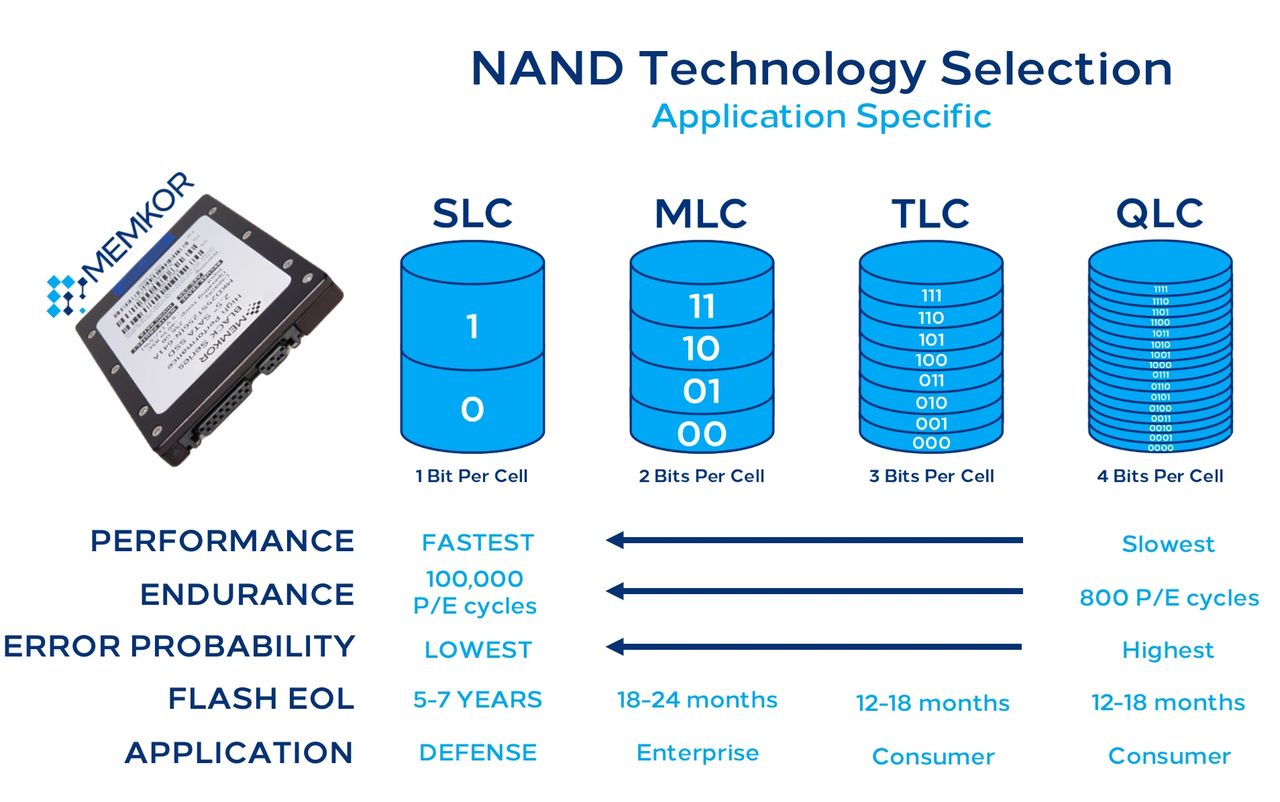
NAND Flash Memory Cell Types: SLC, MLC, TLC & QLC
In NAND flash memory, each cell stores data by trapping electrical charge at different voltage levels. As you pack more bits into a cell, you need more distinct voltage levels, which makes read/write operations more complex and sensitive to errors. Hence, there exist multiple cell structures that differ in the number of bits they can store:
- SLC (Single-Level Cell): Stores 1 bit per cell — simplest and most robust;
- MLC (Multi-Level Cell): Stores 2 bits per cell — a compromise between cost and performance;
- TLC (Triple-Level Cell): Stores 3 bits per cell — very high density;
- QLC (Quad-Level Cell): Stores 4 bits per cell — highest density currently mainstream.
Generally, as you go from SLC ➝ MLC ➝ TLC ➝ QLC, you encounter the following trade-offs:
- Storage density increases (you get more capacity per chip);
- Cost per gigabyte decreases;
- Endurance (write cycles) drops;
- Raw performance (especially write speed) tends to fall.

Summary: Flash Memory Comparison — NOR vs NAND
| Characteristic | NOR Flash | NAND Flash |
|---|---|---|
| Architecture | Parallel cell connections (NOR-like) | Serial cell chains (NAND-like) |
| Access Pattern | True random byte access | Page/block access |
| Read Performance | Fast random reads | Slower random reads, strong sequential |
| Write/Erase | Slower, byte/sector erase | Faster block erase and write |
| Storage Density | Lower density, smaller capacities | Higher density, large capacities |
| Cost per Bit | Higher | Lower |
| Typical Use Cases | Firmware, boot ROM, embedded code | SSDs, memory cards, USB drives |
| Endurance / Lifetime | Higher retention per small capacities | Varies by type (SLC/MLC/TLC/QLC) |
Memory Hierarchy & Practical Trade-offs
As we have seen in the prior sections of this article, no single memory technology does everything perfectly. Instead, modern computers — including mobile devices such as phones and tablets — use a hierarchy of memory types arranged to balance four core factors: speed, cost (in terms of both energy and money), capacity, and whether data persists when power is removed. At the top of the hierarchy are small pools of very fast and volatile memory located close to the processing chip (CPUs, GPUs, TPUs, etc.) in question. Farther down are larger, slower, and eventually non-volatile types used for long-term storage. This arrangement exploits the strengths of each technology while minimizing its weaknesses, as faster and more expensive memories like SRAM and DRAM serve as immediate working storage for a given processor, while persistent technologies such as ROM and flash provide reliable long-term data storage. Organizing memory this way helps systems offer responsive performance for real-time computation while also providing durable storage for large datasets and code.
Below is a table that summarizes the previously discussed and relevant characteristics of each modern computer memory type:
| Memory Type | Volatility | Speed | Density / Cost | Primary Use |
|---|---|---|---|---|
| ROM | Non-volatile | Slow | Moderate / Low cost | Firmware, boot code, etc. |
| SRAM | Volatile | Very fast | Low density / High cost | Processor caches, small buffers, etc. |
| DRAM | Volatile | Fast | Higher density / Moderate cost | System/device memory (RAM, VRAM, etc.) |
| Flash | Non-volatile | Moderate | Very high density / Low cost | Persistent storage (SSDs, USB, SD cards, etc.) |
Future Trends
As modern computing demands continue to skyrocket — driven by artificial intelligence, data centers in the Cloud, IoT devices, and other data-intensive applications — the limitations of today’s mainstream memory technologies are becoming clearer. Accordingly, the semiconductor industry is actively researching what comes next in memory technology, including approaches that blur the line between storage and working memory, improve energy efficiency, or fundamentally redefine how bits are stored and accessed.
Z-Angle Memory (ZAM)
One of the most talked-about emerging technologies is Z-Angle Memory, a novel stacked memory architecture being developed by Intel in partnership with SoftBank’s SAIMEMORY. Designed to challenge current high-bandwidth memory (HBM) by offering greater density, higher bandwidth, and improved energy efficiency, ZAM aims to address the memory bottlenecks in AI accelerators (GPUs and TPUs) and high-performance computing platforms in general. Early development targets commercialization around 2029–2030, with prototypes showcased at industry events marking a shift back toward memory innovation from major players.
Magnetoresistive RAM (MRAM)
MRAM stores data using magnetic rather than electrical states, giving it the rare combination of non-volatility, low latency, and high endurance. Variants like STT-MRAM (Spin-Transfer Torque) and SOT-MRAM (Spin-Orbit Torque) are pushing performance toward SRAM-like speeds while retaining the persistence of flash. A recent breakthrough using tungsten layers reportedly achieved switching speeds on the order of ~1 ns, suggesting MRAM could someday serve as ultra-fast non-volatile working memory with orders-of-magnitude longevity over flash.
Resistive RAM (ReRAM / RRAM)
Resistive Random-Access Memory (ReRAM) uses changes in resistance within a dielectric material to represent bits. It’s attractive because of its simple cell structure, low programming voltage, fast switching, and excellent scalability below 10 nm process nodes, potentially enabling very dense non-volatile storage. Some industry partnerships (e.g., Weebit Nano + Texas Instruments) suggest commercial ReRAM on embedded and IoT devices could finally be close, and its suitability for analog and in-memory computation makes it a candidate for next-gen AI accelerators and edge computing.
Phase-Change Memory (PCM)
Phase-Change Memory (PCM) toggles a chalcogenide material between amorphous and crystalline states using heat, enabling it to store data with much lower latency than NAND flash and better endurance. PCM can leverage multiple intermediate states for multi-bit storage, and unlike DRAM, doesn’t require refresh cycles. Although materials and energy challenges remain, research continues into improving write efficiency and scalability, making PCM a candidate for storage-class memory that sits between DRAM and flash in terms of performance and data persistence.
Ferroelectric & Nano-RAM Approaches
Other experimental technologies aim to combine non-volatility, speed, and endurance in new ways. Ferroelectric flash memory (FeNAND / FeFET-based flash) blends ferroelectric polarization into NAND-like structures to reduce power, expand endurance, and improve speed compared with traditional charge-trap flash cells. Meanwhile, memory concepts like Nano-RAM (NRAM), based on carbon nanotubes, promise DRAM-like speed with non-volatility and potentially very high density. These technologies are at earlier stages but show how materials science and device engineering could drive radical improvements over existing architectures.
Final Words
Memory isn’t just a single component in a computer — it’s a complex ecosystem built from diverse technologies that each make different trade-offs between speed, persistence, cost, and capacity. In this article, we’ve walked through the four major pillars of modern memory: ROM, DRAM, SRAM, and flash, and seen how each serves a unique purpose in making computers work efficiently.
Taken together, these four memory types illustrate a central truth about computing design: no single memory technology excels at every metric, so systems are architected hierarchically to leverage each technology’s strengths while mitigating its weaknesses. From the tiny pieces of firmware stored in ROM to the terabytes of data held on flash, and from SRAM’s blistering speeds to DRAM’s expansive workspace, each form of memory plays a crucial role in the performance and capability of the systems we use every day.
As we look ahead to future innovations — from emerging non-volatile RAMs to advanced stacked architectures — this interplay between performance, persistence, and cost will continue to shape how memory evolves and how we build the next generation of computing devices.


About the author: Sebastian Castellanos is a data scientist by education and training. He's also deeply passionate about PC gaming hardware and software. He has recently started writing technical articles and guides on Wccftech about PC hardware, games and mods.
Follow Wccftech on Google to get more of our news coverage in your feeds.


